Mini LED
01 Basic Concepts
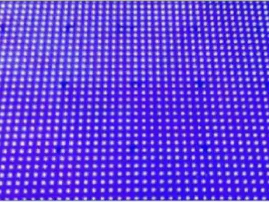
Mini LED refers to LED chips with a size on the order of 100 μm, which is between small-pitch LEDs and Micro LEDs, and is the result of further refinement of small-pitch LEDs. Among them, small-pitch LED refers to LED backlight or display products with the pitch of adjacent lamp beads below 2.5 mm.
Compared with the current mainstream display technology LCD. The mini LED has a better display effect, the response speed has been improved by an order of magnitude, the screen can be thinner, and the power consumption is greatly reduced.
Can extend battery life. Compared with OLED display, mini LED has faster response speed and higher high temperature reliability while maintaining excellent display effect and flexibility.
02 Mini LED application introduction
1. Backlight Mini LED products


2. Direct display Mini LED products

3. Plant lighting Mini LED products

03 Process comparison
1. Technical comparison

2. Equipment Capability - Product Compatibility

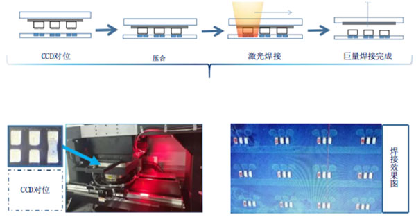
3. Mini LED welding effect

4. Equipment capacity - welding capacity

5. Device lighting effect

The traditional process cannot guarantee the consistency and flatness of the chip surface, resulting in the phenomenon of mura and edge measurement

The mass transfer technology of Keyi Technology adopts the press-fit single-point welding process to effectively ensure the consistency and flatness of the product
surface
. material

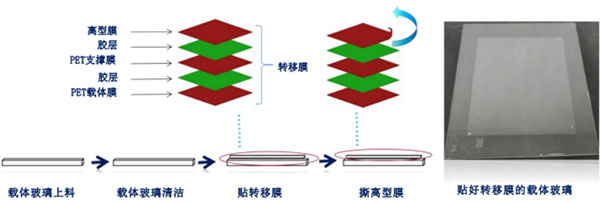
Pasting and tearing film process:

05 Slit type spraying device
Main actions: feeding → flux spraying → discharging

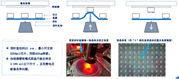
06 Chip arrangement and transfer device
Main actions: feeding→CCD identification→chip arrangement→discharging

Chip Transfer Calibration Process

Schematic Diagram of Transfer Arrangement

07 Chip laser batch welding device
Main actions:
feeding → CCD alignment → pressing → laser welding → discharging

Chip laser batch welding process

08 Test the AOI device.
Main actions: feeding → CCD alignment → optical detection

Electrical testing AOI inspection process:

09 Chip removal device
Main actions: feeding → CCD alignment → laser decrystallization → discharging

Chip Removal Process
 10 Crystal Replenishment Rework Device
Main Actions:
Material Feeding → CCD Alignment → Dispensing and Tin Replenishment → Swing Arm Crystal Replenishment → Laser Welding → Discharging

Crystal rework process:
 11 Automatic transmission device for the whole line
 12 Solution overview
1. Mini LED mass transfer whole line solution

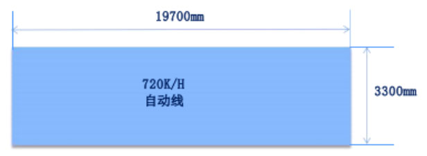
2. Advantages of line layout
Keyi Technology MiniLED mass transfer line
UPH 720K
covers an area of 65㎡
and total energy consumption is 100KWH
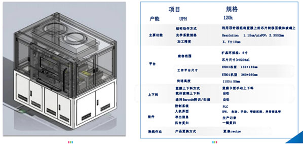
 13 Main parameters

