The transfer of Micro Led to
Mini/Micro-LED as the next-generation new display technology has become the focus of the layout of China's new display industry, and has been vigorously promoted by governments at all levels in terms of policies. Against the backdrop of the gradual recovery of the display industry, Micro-LED is expected to play a leading role in the recovery of the industry as a next-generation display technology, standing at the new outlet of new display applications such as virtual display and vehicle display. It is hoped that the industry will jointly innovate and jointly promote the further development of the global Mini/Micro-LED display industry.
01 Basic concept
The assembly of Micro LED chips usually includes several key process steps, including releasing bulk micro LED chips from the donor/growth substrate (i.e. epitaxial lift-off process), adjusting the pitch size, and finally aligning and moving them to the backplane /Receive substrate (i.e. pick and place process).
Substrate separation: The wafer is separated from the source substrate in batches with a certain force;
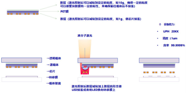
Wafer pick-and-place: The separated Micro LED wafer is selectively picked up from the source substrate with high precision by the transfer device and placed on the target display substrate. on a specific location.
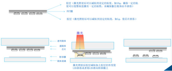
02 Micro LED laser transfer03
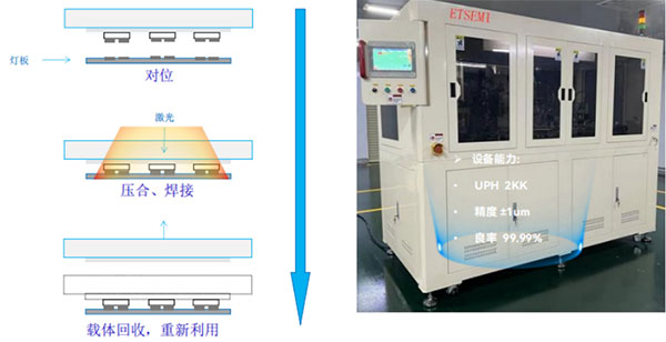
 Micro LED laser welding

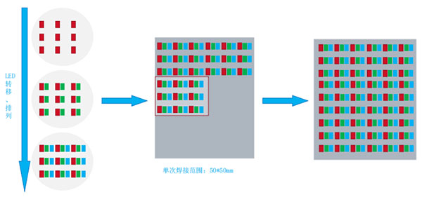
Partition welding of large-size products:

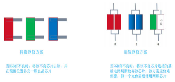
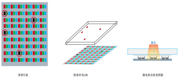
04 LED rework solution
 laser single point repair:
 05 MICRO LED transfer arrangement diagram
 06 MICRO LED transfer welding diagram

07 Process comparison
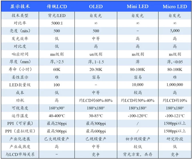
1. Technology comparison

2. Equipment Capability - Product Compatibility

3.Micro LED welding effect

4. Equipment capacity - welding capacity

5. Device lighting effect

The traditional process cannot guarantee the consistency and flatness of the chip surface, resulting in the phenomenon of mura and edge measurement

Keyi Technology's mass transfer technology adopts a pressed single-point welding process to effectively ensure the surface consistency and flatness of the product. 08 The main actions
of the film sticking/tearing device
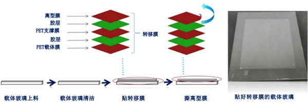
: feeding → glass cleaning → applying transfer film → peel-off film → output material

Pasting and tearing film process:

09 Slit-type spraying device
Main actions: feeding → flux spraying → discharging

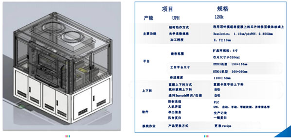
10 Chip arrangement and transfer device
Main actions: feeding→CCD recognition→chip arrangement→discharging

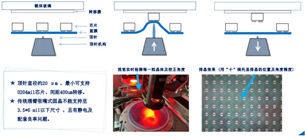
Chip Transfer Calibration Process

Schematic Diagram of Transfer Arrangement

11 Chip laser batch welding device
Main actions:
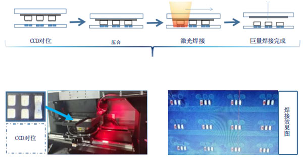
feeding→CCD alignment→pressing→laser welding→discharging

Chip laser batch welding process

12 Test the AOI device
Main actions: feeding→CCD alignment→optical detection

Electrical testing AOI inspection process:

13 Chip removal device
Main actions: feeding → CCD alignment → laser decrystallization → discharging

Chip removal process
 14 Crystal rework device
Main actions:
feeding→CCD alignment→dispensing glue tin repair→swing arm refilling→laser welding→discharging

Crystal rework process:
 15 Automatic transmission device for the whole line
 16 Overview of the scheme
1. Mini LED mass transfer whole line scheme

2. Line layout advantages
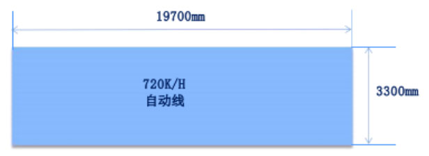
Keyi Technology MiniLED mass transfer line
UPH 720K
covers an area of 65㎡
, total energy consumption 100KWH
 16 main parameters,
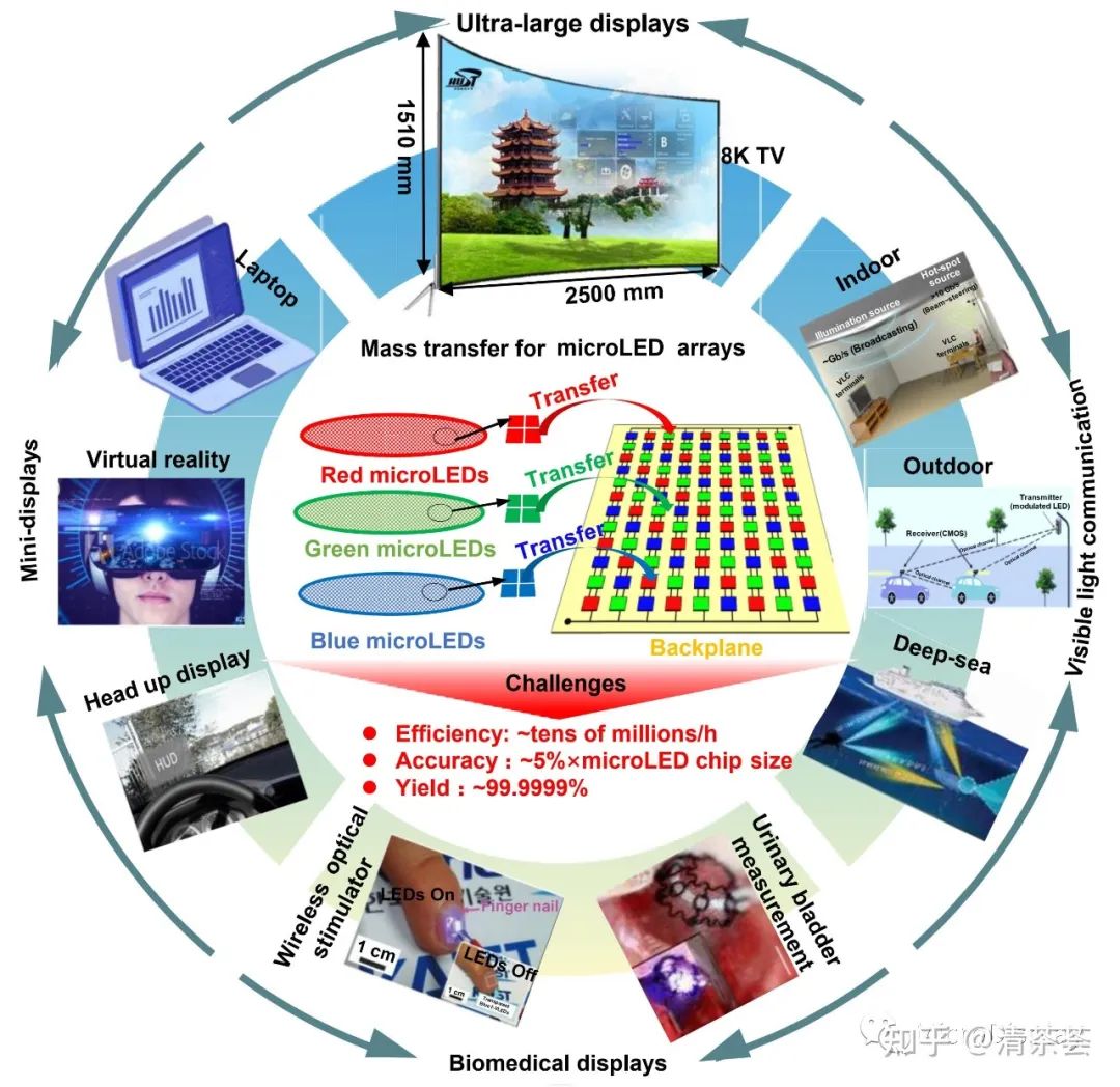
 mass transfer technology is a promising solution that has been proven to overcome the extreme requirements of assembling MicroLED chips. Including laser lift-off technology, contact μTP technology, laser non-contact μTP technology and self-fluid assembly technology, etc.
01Basic Concept
The assembly of MicroLED chips usually involves several key process steps, including releasing the bulk microLED chips from the donor/growth substrate (i.e. epitaxial lift-off process), adjusting the pitch size, and finally aligning and moving them to the backplane/receiver Substrate (i.e. pick and place process).
Substrate separation: using a certain force to separate the wafers from the source substrate in batches; wafer
picking and placing: using a transfer device to selectively pick up the separated Micro LED wafers from the source substrate with high precision and transfer them to the target display substrate. on a specific location.

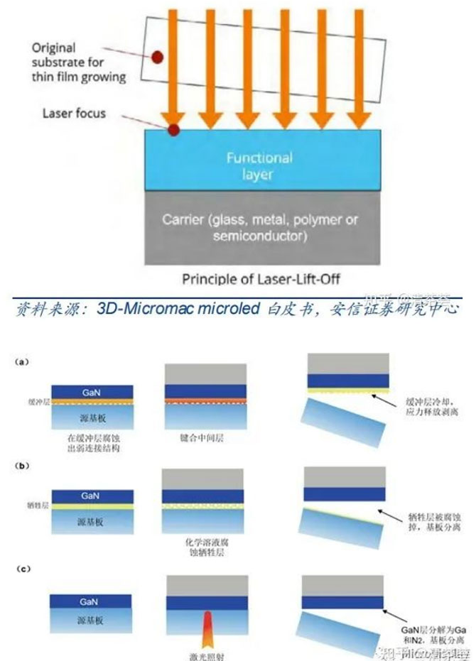
02 Substrate peeling
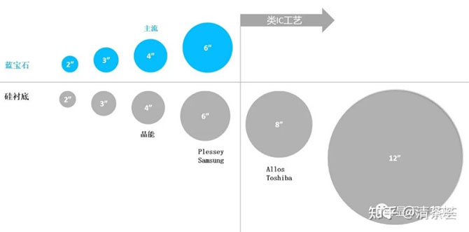
Unlike OLED display technology, inorganic LEDs cannot be produced on large areas on glass or other large-size substrates, so they need to be produced on a semiconductor substrate and then transferred to the driving backplane. The substrate currently used in LEDs is generally sapphire, but the lattice and thermal expansion coefficient between the sapphire and the epitaxial layer do not match. When the size increases, bowing will occur due to stress. Moreover, the sapphire substrate is not compatible with the current large-scale integrated circuit chips, so there are also plans to use silicon as the epitaxial substrate.

Regardless of the substrate form, LEDs require more or less transfer actions when they are made into finished products. Sapphire substrate is currently the mainstream substrate material for Micro LED, but the sapphire substrate is non-conductive and poor heat dissipation will affect the luminous efficiency of Micro LED devices, and brittle sapphire is not conducive to the application of Micro LED in the direction of flexible display, so it is necessary to produce high-resolution For Micro LED chips with high efficiency, high brightness, high contrast, and micro size, peeling off the sapphire substrate is a necessary step.

03 Chip transfer
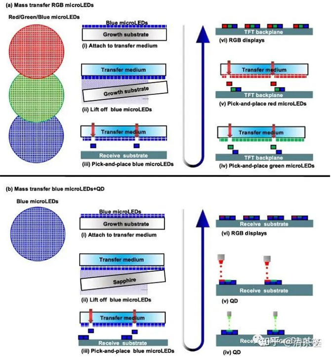
In order to realize full-color MicroLED displays, transfer technologies can be divided into two categories:
the first strategy is the selective batch transfer of RGB MicroLED chips. In the epitaxial lift-off process, MicroLED chips of different colors are separated from their growth substrates. Next, in the pick-and-place process, the transfer medium is used to pick up the RGB MicroLED chips from different growth substrates, followed by placing the RGB MicroLED chips onto the target receiver substrate.
The second strategy is selective bulk transfer of monochromatic Blue/UV MicroLED chips followed by integrated color conversion, such as inkjet printing of quantum dots (QD ) or light-emitting polymers. For high-rate special displays (such as AR), the entire blue microLED chip can be directly transferred immediately after the epitaxial lift-off process (called "monolithic transfer") without changing the original distance between adjacent microLED chips. However, color conversion technology still has some technical problems, such as heat dissipation difficulties, low color conversion efficiency and thermal stability. Therefore, the transfer process remains an essential step until now.
